Contact
search
bars
Company
angle-down
Equipment & Services
angle-down
Technology
angle-down
Applications
angle-down
Careers
angle-down
News & Events
angle-down
Contact Us
angle-down
Equipment & Services
EQUIPMENT
LITHOGRAPHY SERVICES
HOME
angle-right
Equipment & Services
Equipment
We Offer Solutions for Increasing Performance and Efficiency of Photonics Devices.
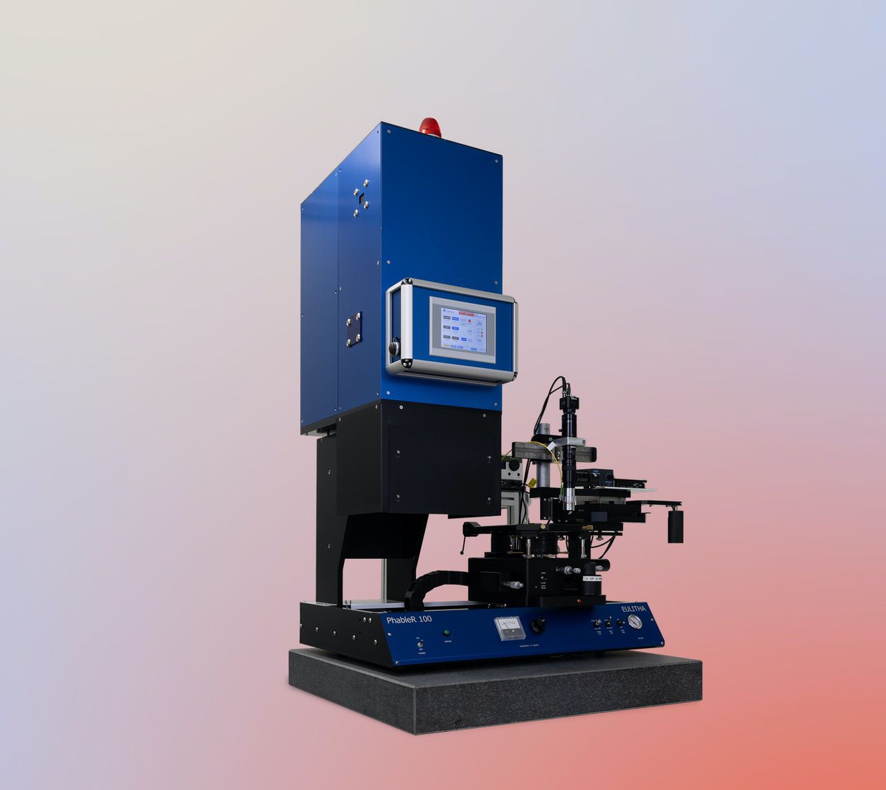
PhableR
R&D and Low Volume Manufacturing of Photonics Patterns.
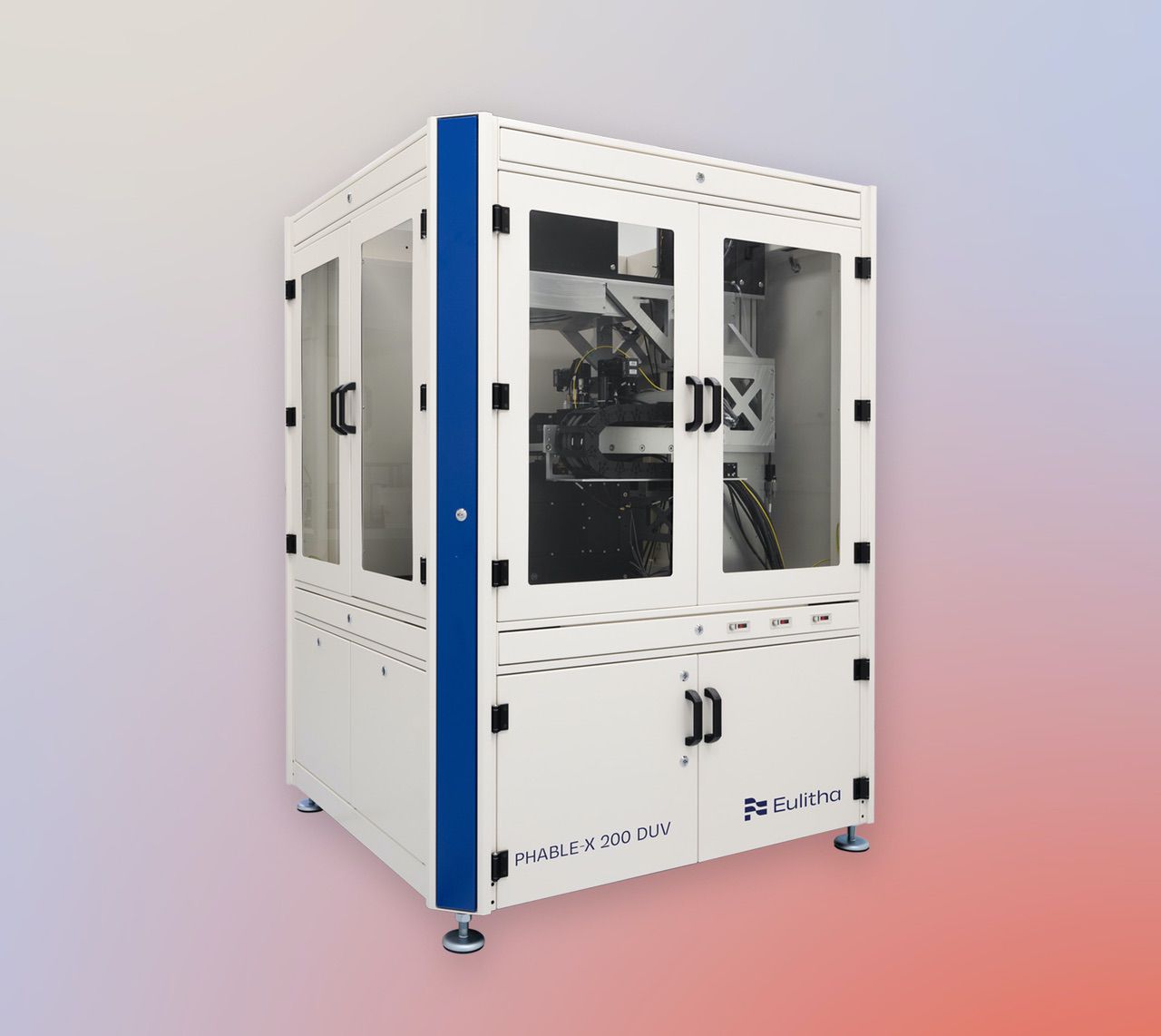
PhableX
Lithography System for Industrial Manufacturing of Photonics Patterns.
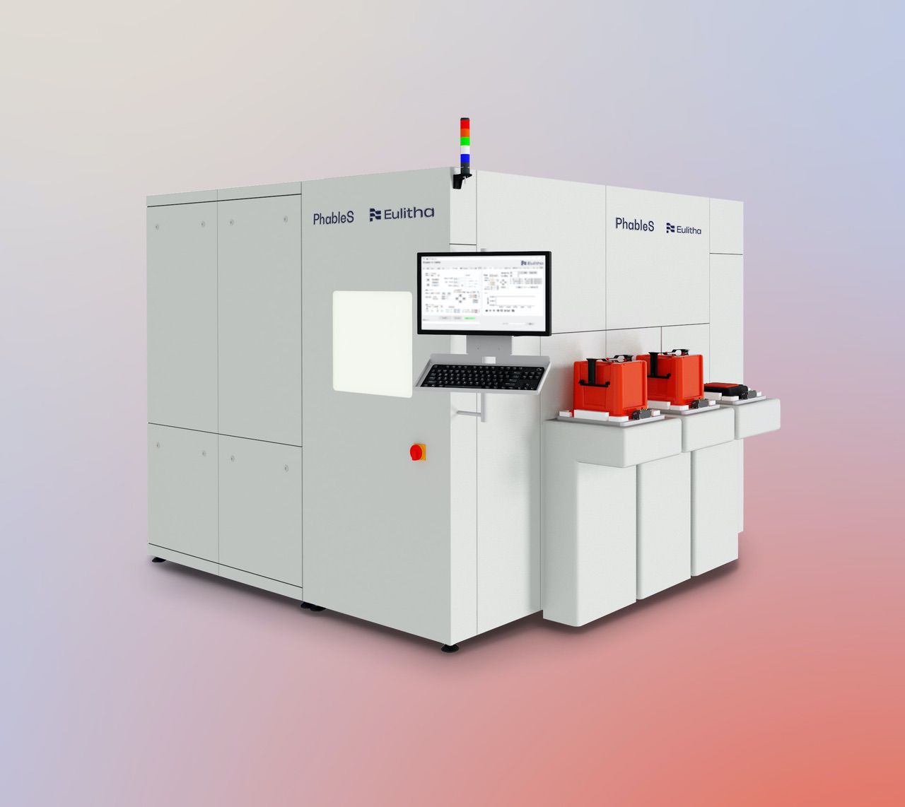
PhableS
Step-and-Repeat Lithography System for Industrial Production of Photonic Patterns.
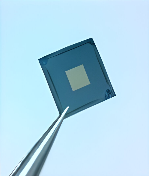
EUV gratings
We offer EUV transmission diffraction gratings patterned on thin silicon or silicon nitride membranes.
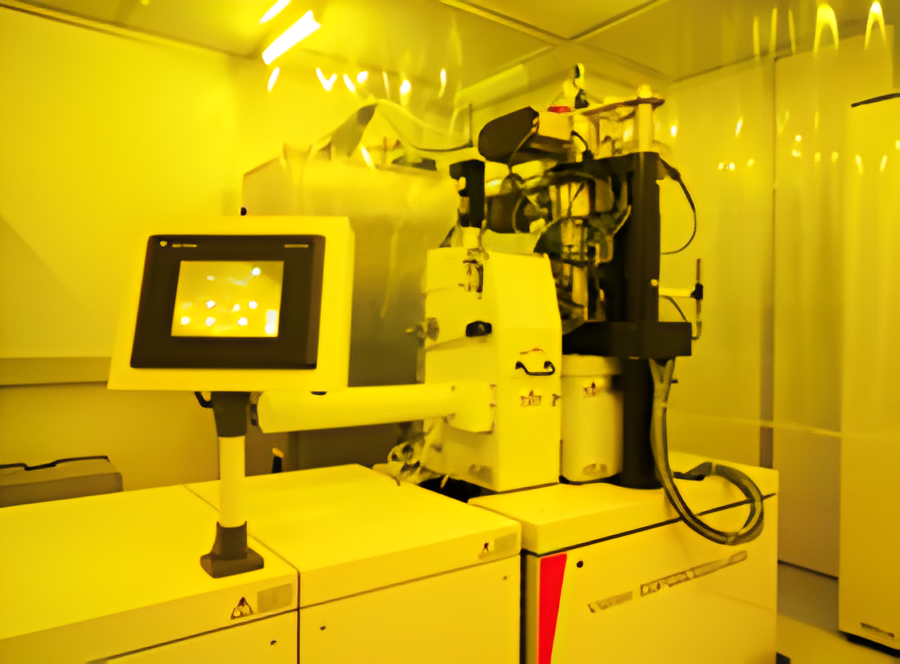
Ebeam Services
EULITHA is making nanostructures with a state-of-the-art e-beam system.
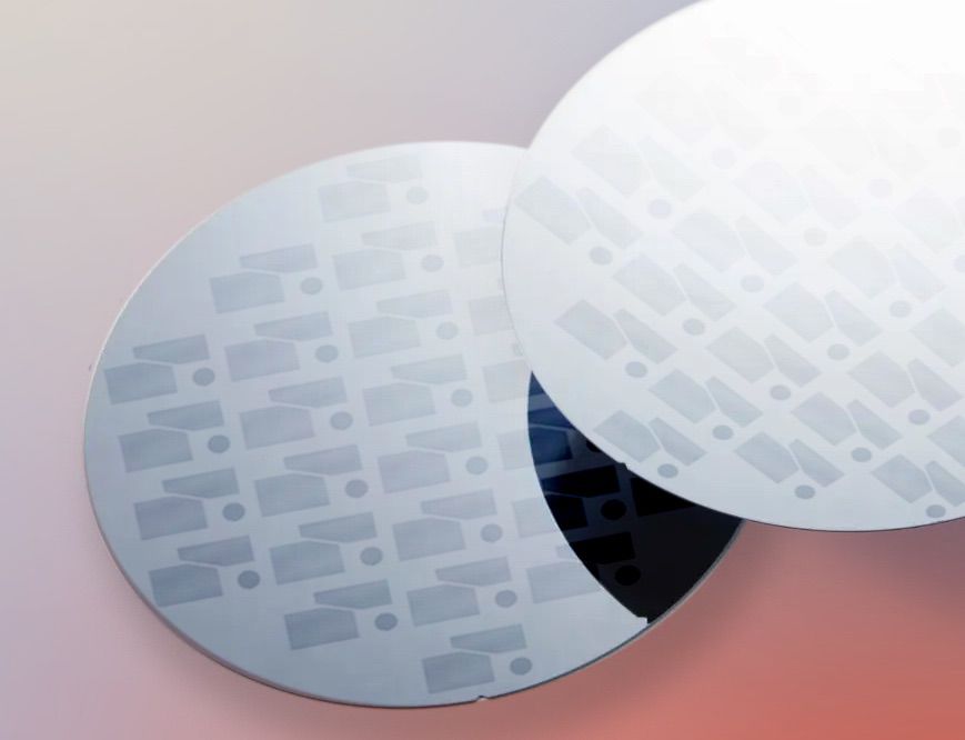
Standard Patterns
Standard line of 1D and 2D periodic nanostructures used in manufacturing of Nanoimprint Templates and other Research and Development projects.
Lithography
Services
We deliver lithography services with a customer-centric approach by performing all steps of lithographic patterning from design of a photomask to the final printing in photoresist to provide you samples and validate your applications.
PhableR
R&D and Low Volume Manufacturing of Photonics Patterns.
PhableX
Lithography System for Industrial Manufacturing of Photonics Patterns.
PhableS
Step-and-Repeat Lithography System for Industrial Production of Photonic Patterns.
EUV gratings
We offer EUV transmission diffraction gratings patterned on thin silicon or silicon nitride membranes.
Ebeam Services
EULITHA is making nanostructures with a state-of-the-art e-beam system.
Standard Patterns
Standard line of 1D and 2D periodic nanostructures used in manufacturing of Nanoimprint Templates and other Research and Development projects.
Photolithography
Application Validation (Demolab)
Custom Nano Patterning
in detail
GET IN TOUCH
Contact Us via Contact Form and We’ll Get Back to You Shortly.
CONTACT US