Products & Services
Standard Patterns
Eulitha uses its unique PHABLETM technology to make the broadest set of periodic nano patterns available in our industry as standard products. This provides research and development groups in both industrial and academic settings access to large area patterns at an affordable cost. Browse our growing selection below and it is likely that you will find patterns closely matching your requirements. And if not, drop us a note and we will look for a solution that may not be on our standard selection yet.
dash dark
DETAILS
Standard Phable™ -made Nanoimprint Templates

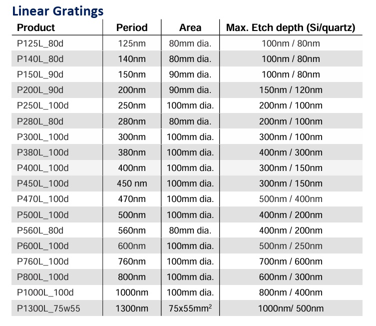
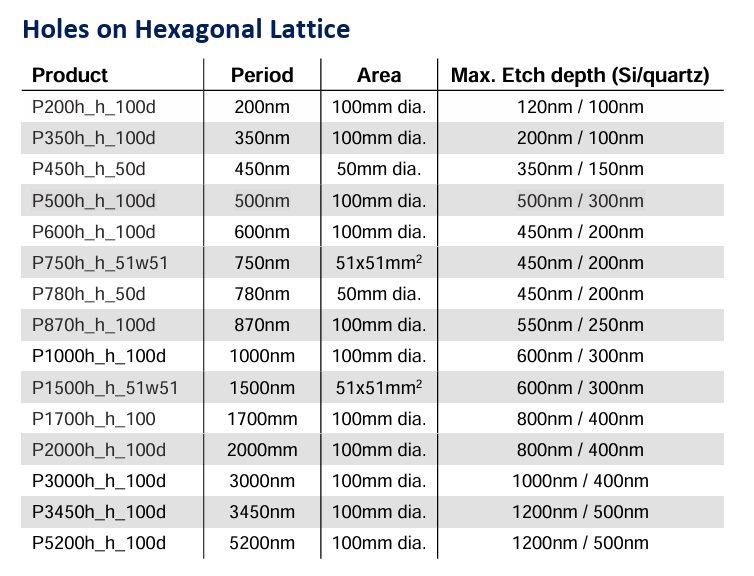
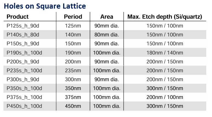
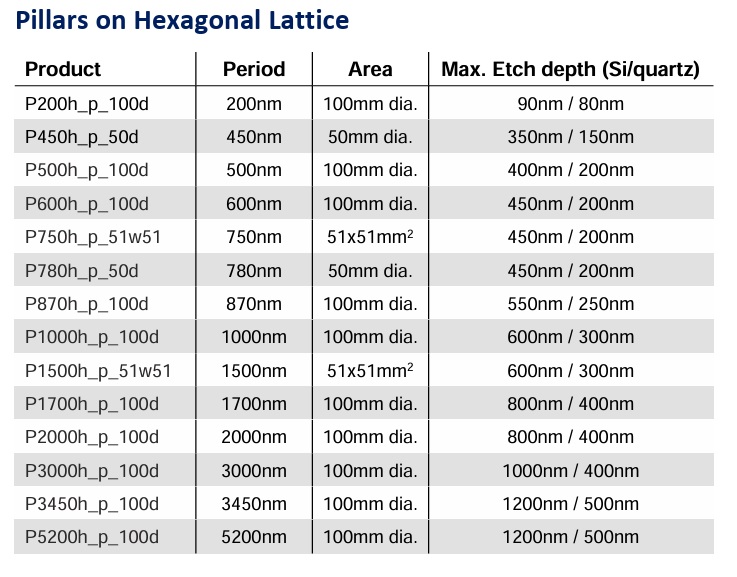
Eulitha’s photonic templates are made with its revolutionary PHABLE™ technology, which guarantees highest quality at an affordable price. Optimized silicon and quartz etching yields hole and pillar patterns with a slight positive slope that facilitates the imprint process. Standard templates with square and hexagonal lattices as well as linear gratings are available.

The applications are almost unlimited including:

  • Nanoimprint process and product development
  • Laser diffraction gratings
  • Plasmonics
  • Antireflection structures
  • Wiregrid polarizers
  • Sensor arrays
  • Templates for crystal growth
  • Research and development

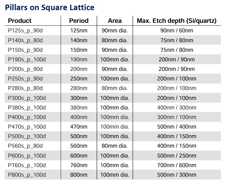
PHABLE™ made Standard Patterns:

  • Photonic templates are provided on 4” Silicon or Fused Silica substrates as standard
  • In most cases these standard patterns can be produced on customer’s own wafers, e.g. as photoresist patterns on GaN or sapphire wafers
  • In certain cases templates on other substrates, e.g. 75mm, 150mm and 200mm wafers are available upon request
  • Dicing to smaller substrate sizes are available upon request
  • Feature (hole or pillar) diameter is about half of the pattern pitch
  • Please inquire, if other duty-cycles, e.g. small pillars or holes, are required
  • Templates are manufactured upon order according to the feature height requested by the customer
  • Inquire for different feature heights that exceed the maximum indicated in the product tables
  • Anti-adhesion coating as well as dicing is available as an option on all NIL stamps
ProductPattern PeriodPattern AreaLinewidthMax. Feature Height
(Si/Quartz)
MP250L300250nm,
275nm,
300nm
7x7mm2 square each90nm/250nm,
100nm/275nm,
120nm/300nm
<200nm / <100nm
MP300L600300nm,
400nm,
500nm,
600nm
10x10mm2 square each135nm/300nm,
175nm/400nm,
250nm/500nm,
300nm/600nm
<300nm / <150nm
MP800L1500800nm,
1000nm,
1200nm,
1500nm
20x20mm2 square each400nm/800nm,
500nm/1000nm,
600nm/1200nm,
700nm/1500nm
<1000nm / <500nm
MP500L2050500nm,
550nm,…,
2000nm, 2050nm
12x12mm2 square each<600nm / <300nm

Multi-Resolution Linear Grating Combinations – Download data sheet
Download data sheet
Download data sheet
Download data sheet
Download data sheet
Download data sheet
SEM image of a 1.3um period v-groove pattern in silicon
High resolution linear grating – 140nm period
Hexagonal array – 600nm pitch
SEM image of a 600nm-period hexagonal array of Au discs
dash
GET IN TOUCH
Contact Us via Contact Form and We’ll Get Back to You Shortly.
CONTACT US
anchor